Multi-channel acquisition core
Synchronized ADC sampling, timestamping, buffering, and USB/Ethernet streaming for compact measurement devices.
FPGA fabric / ADC front end / timing PLL / host bridgeFPGA work
The FPGA side of the lab focuses on practical prototype logic: capture paths, timing adaptation, control IO, board bring-up, and component choices that make the design buildable.
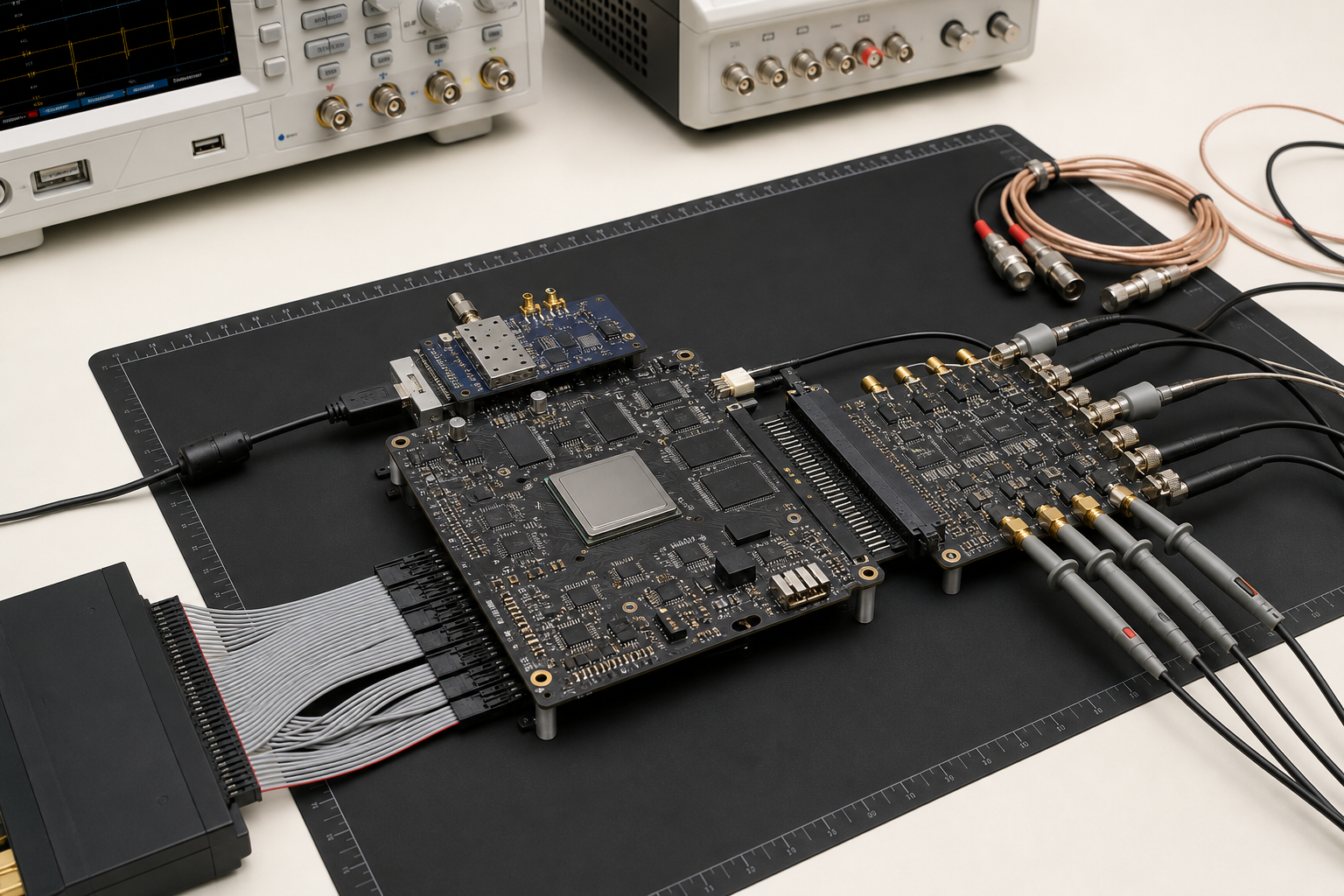
Bench setup
FPGA validation is presented as a measured workflow: clocks, interfaces, capture paths, control timing, and correlation with physical test equipment.
Representative work
Synchronized ADC sampling, timestamping, buffering, and USB/Ethernet streaming for compact measurement devices.
FPGA fabric / ADC front end / timing PLL / host bridgeLow-latency PWM, encoder capture, fault input handling, and isolated gate-driver evaluation for control prototypes.
PWM logic / quadrature decode / isolation / MOSFET driversSensor bring-up, parallel video capture, line buffering, pixel transforms, and measurement hooks for edge-vision devices.
MIPI-style IO study / frame buffers / debug probesBridges between legacy parallel buses, SPI, LVDS-style links, and microcontroller hosts where firmware alone is too slow.
Bus bridge / clock domains / CDC checks / logic analyzer tracesFPGA validation focus
Clock-domain crossing review
ADC/DAC capture and buffering
Low-latency control paths
Parallel bus and protocol bridges
Logic analyzer and oscilloscope correlation
HDL test benches and bench notes