Programmable logic
HDL blocks, timing constraints, clock-domain crossing checks, external memory paths, deterministic IO, and capture pipelines.
Component selection
TDS Electronics Lab helps clients select proper components for custom electronics, FPGA-adjacent hardware, sensors, power stages, and mixed-signal prototypes.
Selection plate
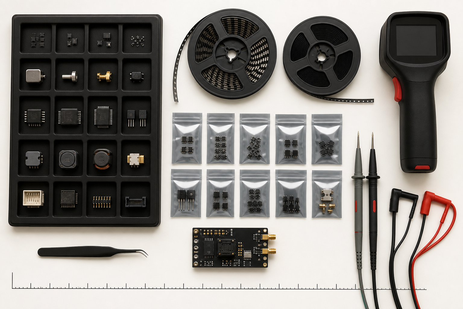
We compare components against the actual circuit goal: signal range, timing, thermal behavior, firmware effort, layout constraints, distributor path, and expected prototype tests.
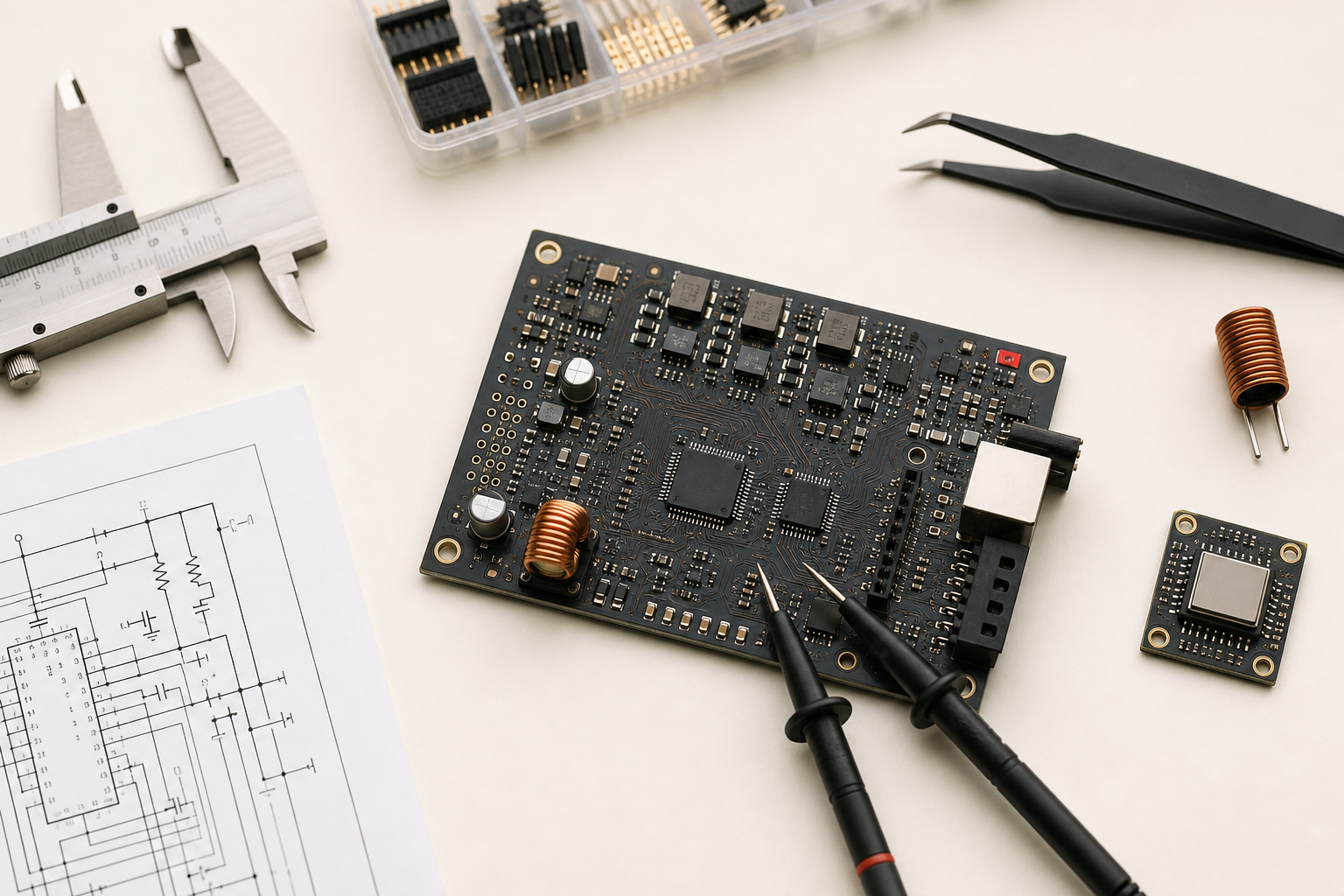
We check package choice, routing pressure, test points, protection, thermal margin, and whether the component keeps the next board spin realistic.
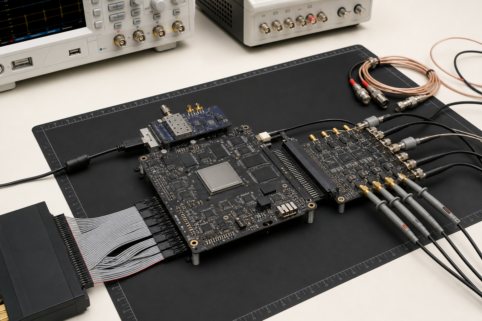
For FPGA-adjacent boards, the selected parts must match clocks, voltage domains, capture paths, connectors, and measurable bench access.
Decision areas
HDL blocks, timing constraints, clock-domain crossing checks, external memory paths, deterministic IO, and capture pipelines.
Bring-up for microcontrollers, secure elements, NFC, CAN, Ethernet, Bluetooth, Matter, and low-power control boards.
Op-amps, ADCs, DACs, isolation, clocks, references, sensor front ends, and mixed-signal noise checks.
MOSFETs, drivers, PMICs, regulators, SiC/GaN candidates, magnetics, protection, and thermal behavior.
Selection focus
MCU, FPGA, and connectivity architecture fit
ADC, DAC, op-amp, reference, and isolation tradeoffs
Power topology, MOSFET, driver, PMIC, and thermal margin
Sensor, connector, ESD, magnetics, and mechanical constraints
Availability, second source, lifecycle, and distributor route
Prototype risk, test access, firmware impact, and BOM cost
Working method
The result is a short engineering decision trail that helps clients understand what to buy, what to avoid, and what to test before the next prototype.
Decision packet
We keep the output practical so the selected parts can move into schematic, purchasing, and bring-up work with fewer surprises.
For clients
Send the target function, current schematic status, critical limits, and the parts you are considering. We will turn it into a practical selection and validation path.