Programmable logic
HDL blocks, timing constraints, clock-domain crossing checks, external memory paths, deterministic IO, and capture pipelines.
Electronics Lab
Commercial prototype lab
We help clients choose the right components for real constraints: availability, electrical fit, firmware impact, layout risk, thermal behavior, and the prototype path to a reliable product.
VHDL / Verilog / timing closure
ADC, DAC, LVDS-style, SPI, USB, Ethernet
PMIC, MOSFET, drivers, thermal checks
component choice, alternates, availability risk
Lab plates
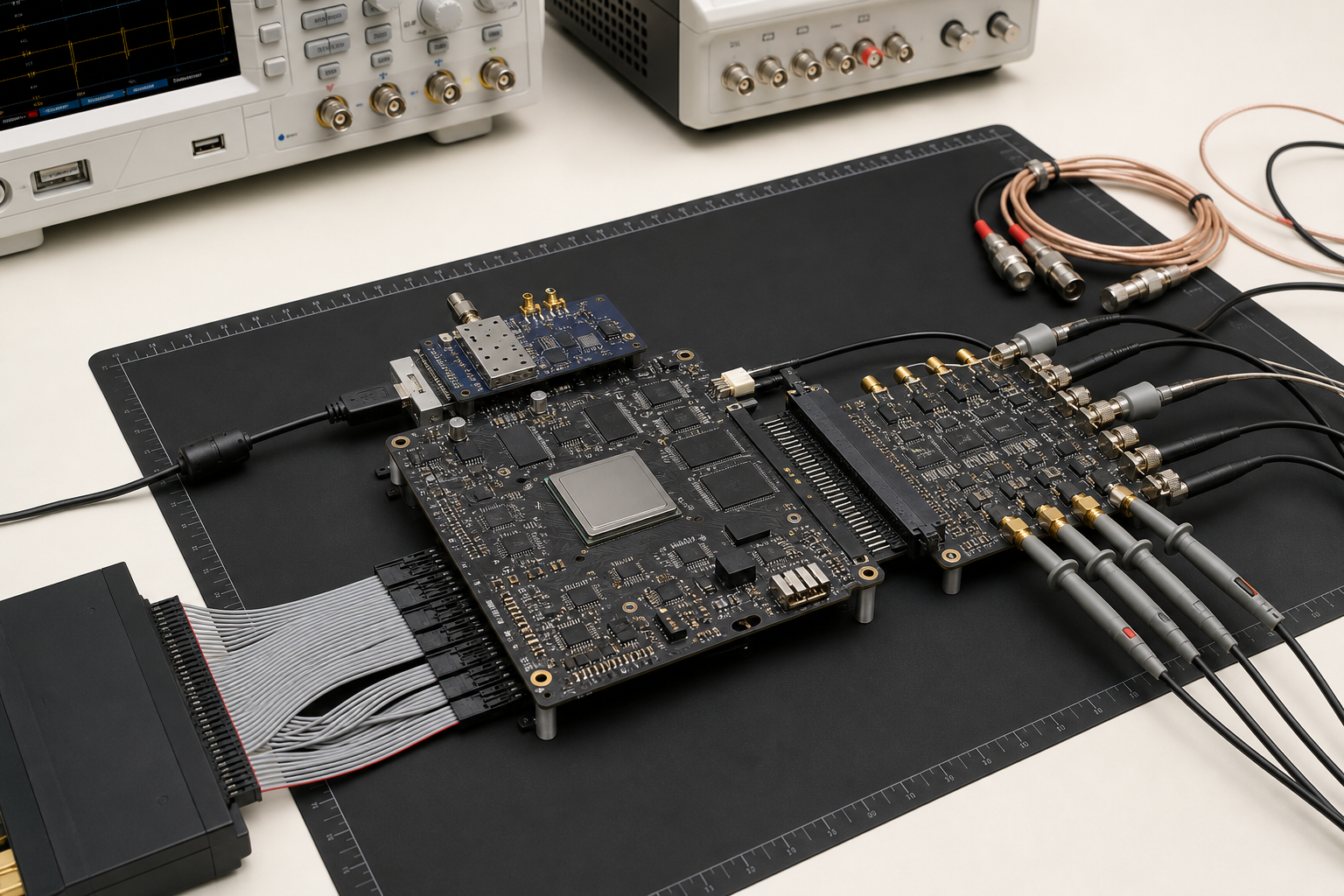
The image system now behaves like a technical sheet: a measured visual plate, a compact explanation, and a scannable proof list.
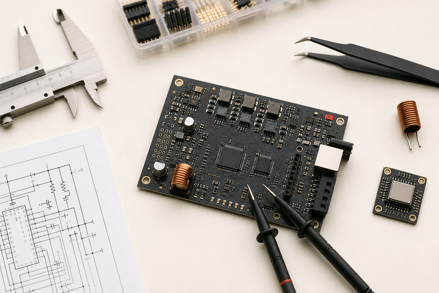
Architecture, schematic decisions, enclosure limits, connectors, power paths, and test access are reviewed before the prototype becomes expensive to change.
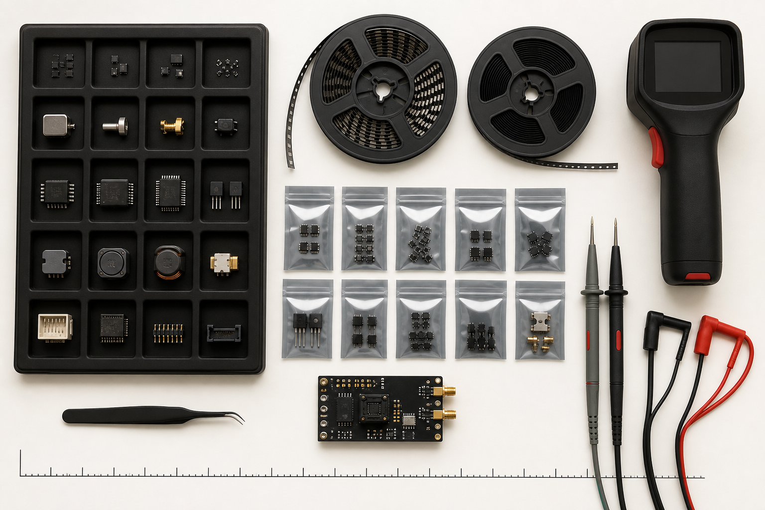
Each recommendation connects the component to the circuit role, firmware impact, layout risk, stock position, and bench checks needed for the next prototype.
Design model
Components are selected inside realistic circuit decisions: layout risk, test access, timing, thermal behavior, firmware touchpoints, lifecycle, and availability.
Component decision capabilities
The lab is set up for practical component decisions: which part fits the design, what risks remain, and which alternate keeps the project buildable before the BOM is locked.
HDL blocks, timing constraints, clock-domain crossing checks, external memory paths, deterministic IO, and capture pipelines.
Bring-up for microcontrollers, secure elements, NFC, CAN, Ethernet, Bluetooth, Matter, and low-power control boards.
Op-amps, ADCs, DACs, isolation, clocks, references, sensor front ends, and mixed-signal noise checks.
MOSFETs, drivers, PMICs, regulators, SiC/GaN candidates, magnetics, protection, and thermal behavior.
Custom and on-demand designs
We design practical electronics around the parts that matter: prototype boards, FPGA logic, power paths, sensor interfaces, and measurement fixtures.
Circuit architecture, component selection, risk review, test point planning, and revision strategy before layout begins.
Compact PCB design guidance for embedded, analog, power, sensor, connector, and FPGA-adjacent electronics.
Focused support for stuck designs: part substitution, signal checks, FPGA feasibility, interface debugging, and redesigns.
Representative FPGA work
These examples show the type of work we can support with component decisions: logic design, high-speed interfaces, mixed-signal capture, power validation, and production-oriented notes.
Synchronized ADC sampling, timestamping, buffering, and USB/Ethernet streaming for compact measurement devices.
FPGA fabric / ADC front end / timing PLL / host bridgeLow-latency PWM, encoder capture, fault input handling, and isolated gate-driver evaluation for control prototypes.
PWM logic / quadrature decode / isolation / MOSFET driversSensor bring-up, parallel video capture, line buffering, pixel transforms, and measurement hooks for edge-vision devices.
MIPI-style IO study / frame buffers / debug probesBridges between legacy parallel buses, SPI, LVDS-style links, and microcontroller hosts where firmware alone is too slow.
Bus bridge / clock domains / CDC checks / logic analyzer tracesComponent selection focus
MCU, FPGA, and connectivity architecture fit
ADC, DAC, op-amp, reference, and isolation tradeoffs
Power topology, MOSFET, driver, PMIC, and thermal margin
Sensor, connector, ESD, magnetics, and mechanical constraints
Availability, second source, lifecycle, and distributor route
Prototype risk, test access, firmware impact, and BOM cost
Decision packet
TDS Electronics Lab gives clients a concise engineering packet: candidates, reasons, alternates, risks, and the validation steps needed before a board spin.
For clients
Send the project goal, current constraints, and the component decisions that are blocking the next prototype step.