Schematic and architecture
Circuit architecture, component selection, risk review, test point planning, and revision strategy before layout begins.
Custom designs
TDS Electronics Lab supports custom boards and redesigns where component choice, testability, supply, and bring-up risk matter as much as the schematic.
Design method
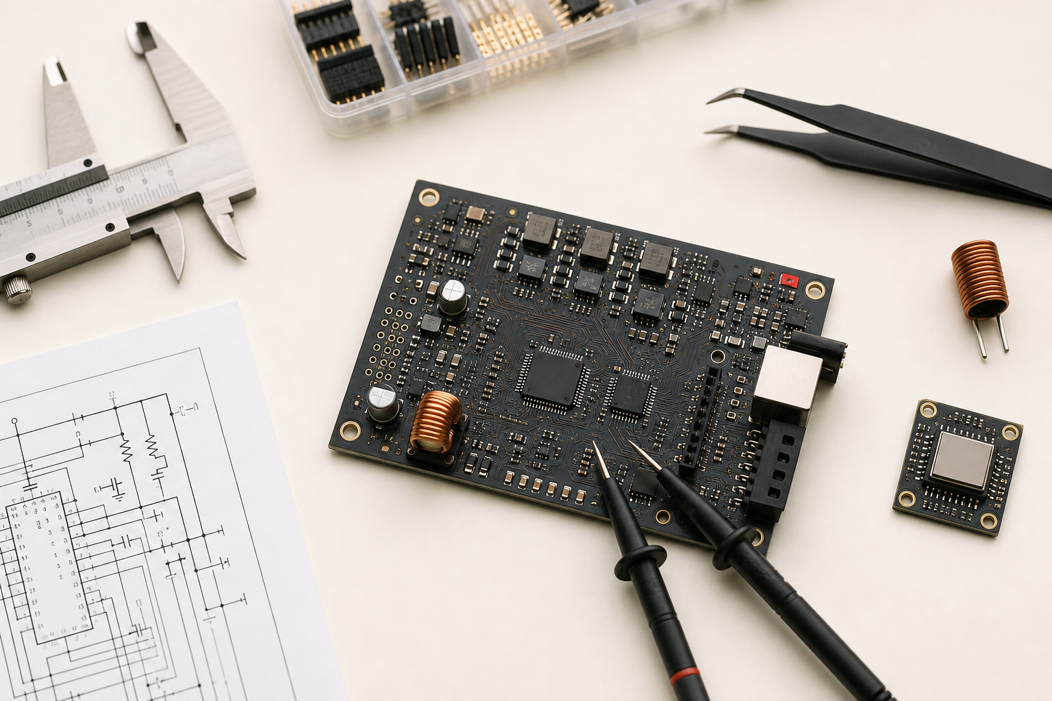
The custom design workflow is built around a clean handoff: architecture, component risk, test access, validation notes, and the next prototype revision.
Design scope
Circuit architecture, component selection, risk review, test point planning, and revision strategy before layout begins.
Compact PCB design guidance for embedded, analog, power, sensor, connector, and FPGA-adjacent electronics.
Focused support for stuck designs: part substitution, signal checks, FPGA feasibility, interface debugging, and redesigns.
Typical deliverables
The output is intentionally practical: enough detail to select parts, debug a prototype, and prepare the next board spin.